

RESEARCH ACTIVITIES
The Department of Applied Sciences which was established in the year 2001 has evolved into a multidisciplinary department which functions in diverse yet complementary fields and helps the students to improve their technological and communication skills. The department encourages research in various fields enabling the faculty members to innovate, create and disseminate knowledge. The faculty members of the department are working in diverse and exciting fields like Chemistry, Physics, Mathematics, Communication Skills, Literature and are involved in continuous up gradation of their knowledge to guide and shape the careers of students in a better way.
The department is currently providing Research Guidance in the fields of:
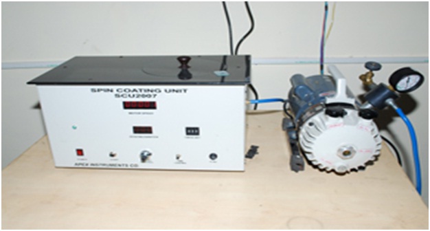
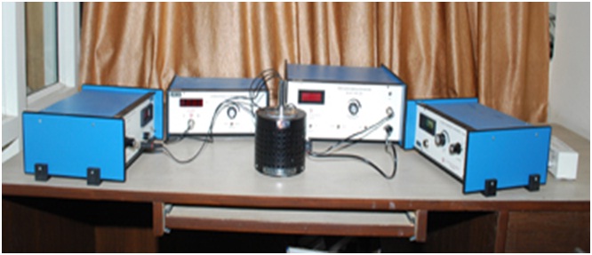
- Microwave Processing.
- Solid Oxide Fuel Cell.
- Nano-materials.
- Heterocyclic Synthesis.
- Medicinal Chemistry.
- Nano chemistry
- Nano-Composites.
- Waste Recycling & Green Chemistry.
- Numerical Analysis.
- Iterative Methods.
- Mathematical Modelling in Ecology.
- Mathematical Modelling in Epidemiology.
- Non-linear dynamical systems.
- Organic chemistry.
- Photo chemistry
- Carbohydrate chemistry.
- Organometallic chemistry.
- Natural products chemistry.
- Natural products chemistry
PATENTS
Patents awarded to the faculty mentioned with details:
| S No. | Name | Title of the invention | Patent no. | Date of Grant |
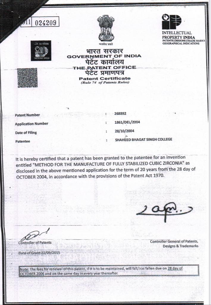
| 1. | Dr. Kanchan L. Singh Dr. Anirudh P. Singh Dr. Navjot Kaur | Manufacturing of Fully Cubic Zirconia at Low Temperature using Microwave Energy | 268892 | 22/09/2015 |
| 2. | Dr. Kanchan L. Singh Dr. Sonia Mago Dr. Payal Sharma Dr. Anirudh P. Singh | A process for preparing YZT a mixed conductor | 419790 | 31/01/2023 |
| 3. | Dr. Anirudh P. Singh Dr. Chetan Sharma Dr. Kanchan L. Singh | A Process for Preparation of Lanthanum Germanium based Apatite Electrolytes |
365133 | 22/04/2021 |
RESEARCH GUIDANCE
| Sr. No. | Name of Faculty | M.Tech. Thesis Guided | Ph.D. Thesis Guided | Ph.D. These Guiding |
| 1 | Dr. Kanchan L. Singh | 10 | 6 | 1 |
| 2 | Dr. Ashok Kumar | 5 | 1 | … |
| 3 | Dr. Rajni Sharma | … | 3 | 2 |
| 4 | Dr. Amit Sharma | … | 1 | 1 |
| 5 | Dr. Shivani Vij | … | 1 |
| Sl. No. | Name of Scholar | Title of Thesis | Name of the University | Year of Award |
| 1 | Payal Sharma 1211005 | Effects of microwave processing on the properties of zirconia and ceria system as electrolytes for solid oxide fuel cell | IKG PTU, Kapurthala | Awarded 2019 |
| 2 | Sonia Mago 1111015 | Fabrication and Characterization of Microwave Processed Anode Materials for Solid Oxide Fuel cell | IKG PTU, Kapurthala | Awarded 2019 |
| 3 | Ravinder Chadha 1212001 | Synthesis of appetite for application as biomaterials | IKG PTU, Kapurthala | Awarded 2021 |
| 4 | Ashwani Chauhan 1311019 | Development of perovskite solar cell | IKG PTU, Kapurthala | Awarded 2020 |
| 5 | Chetan Sharma 1412005 | Fabrication of apatite based electrolyte for solid oxide fuel cell” | IKG PTU, Kapurthala | Awarded 2021 |
| 6 | Manokamna 1412014 | Preparation of Cathode Materials for Solid oxide Fuel cell | Dept of Physics, IKG PTU | Awarded June 2023 |
| 7 | Saloni Sharma 1511003 | Tailoring and characterizing the properties of polyanyline-pvc composites for microwave absorbers | IKG PTU, Kapurthala | Thesis Submitted |
Under the Guidance of Faculty from Department of Applied Sciences, The students of M. Tech. Nano Science and Technology have completed their dissertation work at DAVIET research centre in association with reputed National Research Centre: CSIO, Chandigarh; SSPL, New Delhi; PU, Chandigarh; GNDU Regional Centre, Jalandhar. The students of 2K10 batch had worked on the following topics for their six month dissertation programme:
| Research Work | “Synthesis and Characterization of Nano-Sized NiO-YSZ Composite: A Precursor of Ni-YSZ Anode for SOFC” |
| Faculty | Dr. Kanchan L. Singh, Associate Professor & Head Nanoscience & technology |
| Status: | Executed |
| Research Work | “Investigation of Electronic Properties of DNA Bases for Use in Molecular Electronic Devices” |
| A Poster of the Research. | 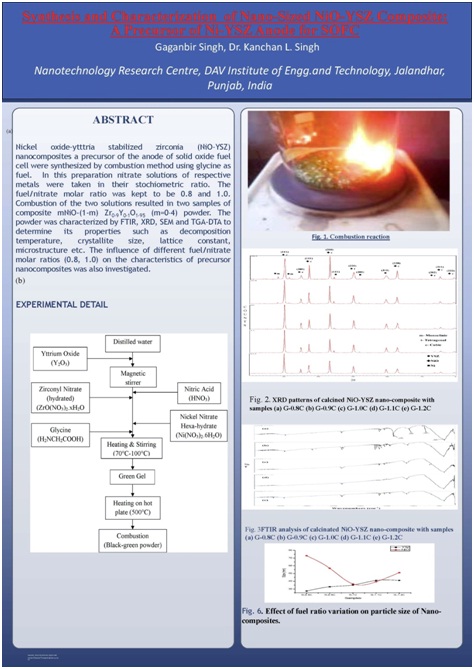 |
| Faculty | Dr. Kanchan L. Singh, Associate Professor & Head Nanoscience & technology |
| Status: | Executed |
| Research Work | “Electrodeposition of Graphene on Silicon for Biosensensing Application” |
| Faculty | Dr. Rupesh Kumar, Assistant Professor, Department of Applied Sciences |
| Status: | Executed |
| Research Work | “Structural and optical characterization of chemically synthesized nanocrystals and thin films of ZnS” |
| Faculty | Dr. Kanchan L. Singh, Associate Professor & Head Nanoscience & technology and Dr. Praveen Kumar, Assistant Professor, Nanotechnology Research Centre |
| Status: | Executed |
| Research Work | “Electrodeposition of Graphene on Silicon for Biosensensing Application” |
| Faculty | Dr. Rupesh Kumar, Assistant Professor, Department of Applied Sciences |
| Status: | Executed |
| Research Work | “ Theoretical Study of the Electronic Properties of Graphene using ATK Simulation” |
| Faculty | Dr. Ashok Kumar, Associate Professor & Head, Department of Applied Sciences |
| Status: | Executed |
| Research Work | “Growth and Structural Characterization of CVD Grown Carbon Nanotubes” |
| Faculty | Dr. Praveen Kumar, Assistant Professor, Nanotechnology Research Centre |
| Status: | Executed |
| Research Work | “Sol-Gel Processing of (Cd, Mg) Co-Doped ZnO Thin Films as Transparent Conductor for Opto – Electronics” |
| Faculty | Dr. Praveen Kumar, Assistant Professor, Nanotechnology Research Centre |
| Status: | Executed |
|
Research Work |
“Detection of urea using graphene Platellets” |
| Faculty | Dr. Kanchan L. Singh, Associate Professor & Head Nano-science & technology and Dr. Praveen Kumar, Assistant Professor, Nanotechnology Research Centre |
| Status: | Executed (In Collaboration with CSIO, Chandigarh) |
|
Research Work |
“Synthesis and Characterization of ZnSe Nano Crystals” |
| Faculty | Dr. Rupesh Kumar, Assistant Professor, Department of Applied Sciences |
| Status: | Executed (In Collaboration with CSIO, Chandigarh) |
|
Research Work |
“Synthesis and Characterization of ZIFs based Porous Nano Materials” |
| Faculty | Dr. Rupesh Kumar, Assistant Professor, Department of Applied Sciences |
| Status: | Executed (In Collaboration with CSIO, Chandigarh) |